For chip implementation of specified algorithms or logic functions, a variety of design styles can be considered. Each design style has its own advantages and disadvantages, so designers must make an informed decision in order to provide functionality at a low cost.
Field Programmable Gate Array (FPGA)
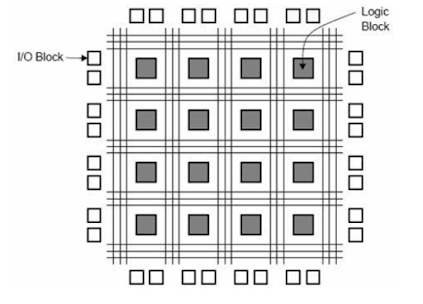
The full form of FPGA is “Field Programmable Gate Array”. It s made up of tens of thousands to millions of logic gates with programmable interconnection. Programmable interconnections are available for users or designers to perform given functions easily. A typical model FPGA chip is shown in the given figure. There are I/O blocks, which are designed and numbered according to function. For each module of logic level composition, there are CLB’s (Configurable Logic Blocks).
CLB executes the logic operation that the module has been provided.The inter connection between CLB and I/O blocks are made with the help of horizontal routing channels, vertical routing channels and PSM (Programmable Multiplexers).
The complexity of the FPGA is solely determined by the amount of CLB it comprises. VHDL or another hardware description language is used to design the features of CLBs and PSM.After programming, CLB and PSM are placed on chip and connected with each other with routing channels.
Advantages:
Starting with the design process to functional chip, it takes very little time.
It does not require any physical manufacturing measures.
The only drawback is that it is more expensive than other models.


Comments
Post a Comment